

India’s semiconductor journey, beginning in the 1980s with SCL in Mohali, has evolved from early ambitions in fabrication to becoming a global design and manufacturing hub. Over the decades, the country shifted focus from developing mature-node chips to supporting assembly, testing, advanced packaging, and design innovation, driven by domestic electronics demand, trade considerations, and policy support. Strategic initiatives like the India Semiconductor Mission (ISM), skill development programs, and international collaborations now anchor an integrated ecosystem that balances market relevance, execution readiness, and long-term sustainability, positioning India as a growing contributor to the global semiconductor landscape.
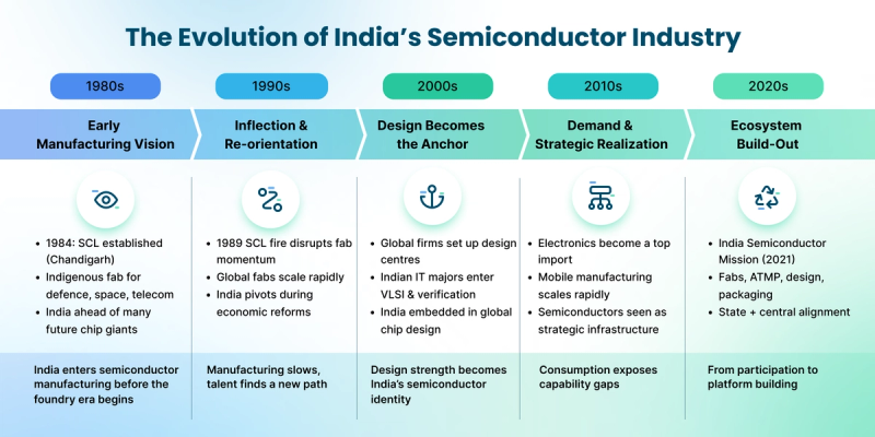
The First Step: SCL and the Vision of the 1980s
India’s semiconductor story formally began in 1984 with the establishment of Semiconductor Complex Limited (SCL) in Chandigarh. The mandate was focused and strategic: develop indigenous semiconductor manufacturing capability for sectors such as space, defence, and telecommunications.
At that time, semiconductor fabrication was still concentrated among a limited number of countries. Dedicated foundry models were rare. Taiwan Semiconductor Manufacturing Company (TSMC), which later became the world’s largest contract chip manufacturer, was founded only in 1987. India’s early entry placed it among a small group of nations attempting end-to-end chip fabrication.
SCL started with fabrication technologies suited to the era and gradually improved process capability. By the late 1980s, it had moved from 5‑micron technologies toward sub‑micron nodes, supplying chips primarily for government and research use. India had strong academic institutions, a trained engineering base, and early electronics demand aligned with this effort.
A Turning Point That Changed the Trajectory
In 1989, a major fire damaged SCL’s fabrication facility, disrupting operations at a critical moment. Semiconductor manufacturing depends on uninterrupted process upgrades, stable infrastructure, and sustained capital investment. The disruption slowed progress just as global semiconductor technology cycles began accelerating.
During the early 1990s, semiconductor manufacturing worldwide entered a phase of rapid scale expansion. Fabrication plants became more capital intensive, technology nodes advanced quickly, and long‑term investment alignment became central to competitiveness. India’s semiconductor pathway adjusted during this period, influenced by broader economic reforms and shifting industrial priorities.
The 1990s: Design Talent Takes Center Stage
While fabrication momentum slowed, India’s software and IT services sector expanded rapidly through the 1990s. This growth created a natural bridge into semiconductor design and embedded systems, where software skills played a critical role.
Global semiconductor companies began establishing design and R&D centres in India, drawn by engineering depth and system‑level expertise. Indian firms such as TCS, Wipro, and Infosys expanded into VLSI design services, verification, and electronics R&D. By the end of the decade, India had become an important contributor to global semiconductor design workflows, even as domestic fabrication activity remained limited.
This phase defined a durable strength. Design capability became the anchor of India’s semiconductor identity for the next two decades.
The 2000s: A Design Hub in a Global Supply Chain
During the early 2000s, India deepened its role as a global semiconductor design hub. Multinational firms expanded captive design centres, and thousands of Indian engineers worked on processors, communication chips, memory controllers, and system‑on‑chip architectures deployed worldwide.
At the same time, East Asian economies invested heavily in fabrication capacity. Taiwan, South Korea, and later China built large‑scale fabs supported by coordinated industrial policy and infrastructure development. Semiconductor manufacturing became central to their technology and export strategies.
India’s electronics market continued to expand, driven by computing devices, telecom infrastructure, and industrial electronics. Semiconductor consumption grew steadily, supported mainly through global supply chains. The gap between strong design capability and limited domestic manufacturing became more visible during this phase.
The 2010s: Electronics Expansion and Policy Alignment
As electronics adoption grew across telecommunications, automotive systems, medical devices, and consumer electronics, semiconductor demand in India rose sharply. Mobile phone production expanded rapidly, and assembly operations spread across multiple states, positioning India as one of the world’s largest mobile phone manufacturing hubs. This growth underscored the central role of semiconductors across the electronics value chain, from chips and components to packaging and testing, emphasizing the need for deeper domestic capability.
At the same time, semiconductors gained strategic importance globally for economic resilience, advanced technology, and national security. India responded by strengthening its electronics and semiconductor policy framework. The Electronics System Design and Manufacturing (ESDM) sector expanded steadily, supported by domestic demand, export opportunities, and skill development initiatives. Research across IITs, IISc, and national laboratories advanced work in nanoelectronics, compound semiconductors, MEMS, sensors, and power electronics, laying technical groundwork for future manufacturing.
This decade combined market growth with policy action, creating institutional learning and industry-academia linkages that would later support large-scale semiconductor ecosystem development.
Learning from Earlier Phases
India’s semiconductor journey reflects interconnected stages, early manufacturing ambition, design‑led growth, and renewed focus on physical production. Each stage informed the next.
Global experience showed that semiconductor ecosystems thrive through sustained capital commitment, coordinated policy execution, talent depth, and supply‑chain integration. These lessons shaped India’s contemporary approach, which emphasizes ecosystem building across design, fabrication, assembly, testing, and materials.
The Current Phase: Building at Scale
The shift toward semiconductor manufacturing in the early 2020s grew out of a clear economic signal. Electronics had become one of India’s largest import categories, with semiconductors forming a growing share of that dependence. This imbalance brought supply security, domestic value addition, and trade stability into sharper focus, elevating chips from a technology concern to an economic priority.
Manufacturing efforts therefore centered on mature and specialty nodes that support automobiles, industrial systems, telecom networks, and consumer electronics, the segments driving most domestic demand. These technologies align with India’s market scale, move faster to volume production, and connect naturally with assembly, testing, and packaging. The emphasis reflects manufacturing readiness and sustained demand rather than competition at the most advanced logic nodes.
The India Semiconductor Mission (ISM) translated this direction into execution by supporting fabrication, advanced packaging, and assembly, alongside incentives for chip design. The approach links India’s design depth with manufacturing that serves current consumption patterns, creating a base for scale, resilience, and ecosystem growth.
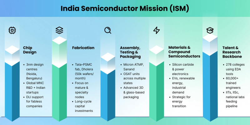
Manufacturing, Packaging, and New Technologies
This strategy is now visible on the ground. India’s semiconductor build-out spans fabrication, assembly, testing, and advanced packaging, reinforcing an ecosystem approach over a single technology bet. Early investments in packaging and mature-node manufacturing signal a focus on capabilities that scale quickly and integrate with global supply chains.
Projects such as Micron’s packaging facility in Gujarat and Tata Electronics’ fabrication partnership in Dholera act as reference points, combining domestic manufacturing with established international expertise. At the same time, rising activity in assembly, testing, and compound semiconductors shows attention to segments where India can build depth across the value chain.
Design continues to anchor this transition. The expansion of advanced design work alongside manufacturing reflects an effort to connect architectural capability with physical production. Together, these elements point to an integrated semiconductor ecosystem shaped by market relevance, execution readiness, and long-term sustainability.
Skills and Research as System Enablers
Talent development forms a central pillar of India’s semiconductor strategy. By 2025, 278 colleges were using advanced EDA tools, and around 60,000 engineers had received semiconductor‑focused training. Student‑driven innovation has also progressed, with 20 chips from 17 institutions fabricated through national programs.
The government has outlined plans to train 85,000 engineers over the next decade. Initiatives such as the SMART Lab at NIELIT Calicut and partnerships with Lam Research, Micron, IBM, and Purdue University link academic training with industrial requirements and global standards.
Global Engagement Through SEMICON India
India’s growing semiconductor role is reflected in SEMICON India, a flagship platform organized under ISM in partnership with SEMI.
SEMICON India 2025 hosted 300+ exhibiting companies from 18 countries, with international pavilions from Japan, South Korea, Singapore, and Malaysia, alongside country roundtables, workforce development programs, and a semiconductor design startup pavilion. The scale of participation reflects India’s growing integration into the global semiconductor network.
Recent Momentum and the Road Ahead
Several developments during 2025 reflected a clear shift from policy intent to on-ground execution in India’s semiconductor journey. The approval of the HCL–Foxconn joint venture in Jewar pointed to progress in building domestic chip manufacturing capability, while announcements around indigenous chip readiness signaled movement across multiple projects rather than isolated efforts. At the same time, state-led electronics initiatives and continued momentum in semiconductor design startups showed growing alignment between manufacturing ambitions and India’s established strengths, reinforcing the foundation of a more integrated semiconductor ecosystem.
Looking ahead, the Union Budget 2026 introduced India Semiconductor Mission 2.0, expanding the focus to equipment manufacturing, semiconductor intellectual property, and resilient supply chains. This next phase signals a shift from early capacity building to ecosystem scale and long-term competitiveness.
India’s semiconductor journey now reflects a connected arc, from strategic need and policy intent to manufacturing capacity, design depth, and global engagement. As these elements continue to mature together, India is positioning itself as a stable and integrated contributor to the global semiconductor landscape.