

At micron scales, tiny machine drift can silently erode yield during wafer test. This article shows how AI turns probe marks into real-time feedback, enabling autonomous prober realignment in milliseconds—preventing latent defects, improving uptime, and stabilizing yield as tolerances shrink.
By Ayaz Aslam | 27th Jan 2026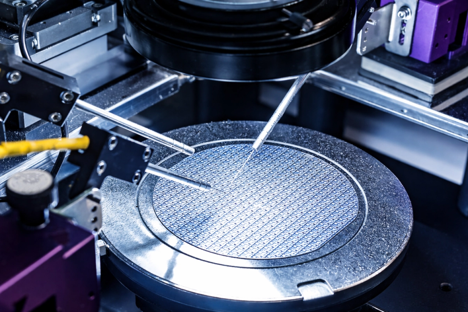
SixSense’s AI-ADC platform integrates with inspection and DMS systems to automate defect classification at production scale. Deployed across leading foundries and OSATs, it processes millions of inspection images annually. The platform is now expanding into real-time classification and fab-wide deviation control.
By Avni Agrawal | 22nd Jan 2026
Manufacturing downtime is becoming more costly and complex in the Industry 4.0 era. This blog explains how AI-driven root cause analysis helps manufacturers move beyond reactive troubleshooting to identify true causes across inspection, metrology, FDC, and test data. Learn how AI-powered RCA reduces downtime, improves yield, and strengthens overall operational performance.
By Vicknes Ratha Kishnan | 20th Jan 2026

SixSense delivered major AI milestones in June, expanding semiconductor and HDD manufacturing deployments with higher yield, AI-powered defect classification, inspection automation, and accelerated model deployment. From earning World Economic Forum Technology Pioneer 2026 recognition to achieving over 90% automation with zero inspection escapes in advanced packaging, SixSense continues advancing production-grade AI for wafer fabs, OSATs, and HDD fabs.
Prakriti Chaturvedi25th Jun 2026
A wafer-level bumping and RDL manufacturer achieved 98% defect classification accuracy using only 200 curated images, outperforming a model trained on 20,000 images. Learn why image selection, label quality, and AI-powered data preparation matter more than dataset size in semiconductor inspection.
Prakriti Chaturvedi24th Jun 2026
AI-powered defect classification at AIT inspection transforms HDD head manufacturing by reducing false alarms, preventing over-inking, and catching critical defects before they escape downstream. By converting 100% of optical inspection data into actionable yield intelligence, fabs can improve baseline yield, accelerate excursion detection, and unlock millions in annual savings.
Prakriti Chaturvedi24th Jun 2026
SixSense expanded its AI deployments across advanced packaging and wafer fabs in May 2026, helping semiconductor manufacturers improve yield, automate defect inspection, and accelerate root cause analysis. At a leading OSAT, SixSense AI-ADC achieved >99.8% yield, zero escapes, and over 90% review automation in high-volume production. SixSense also showcased its AI-RCA and semiconductor AI innovations at SEMICON Southeast Asia 2026 and ASMC 2026, highlighting the growing role of AI in yield engineering and process control.
Prakriti Chaturvedi21st May 2026
AI-powered Root Cause Analysis is transforming semiconductor manufacturing by reducing fab investigation time from days to hours. By connecting SPC, MES, defect, and equipment data, AI helps fabs identify root causes faster, reduce yield loss, improve tool productivity, and scale engineering knowledge across advanced semiconductor fabs.
Prakriti Chaturvedi15th May 2026
10 production models. >90%+ automation. 0% escapes. >99.8% Yield
Prakriti Chaturvedi15th May 2026
Most of the public debate around AI hardware is about GPU design, but the harder constraint right now is one step further down the supply chain. A small number of facilities in Taiwan and South Korea handle almost all of the advanced packaging that turns silicon into finished AI systems, and they have been sold out for over a year.
Prakriti Chaturvedi12th May 2026
A plain-English guide to flip chip, fan-out, 2.5D, and 3D, and why they matter for AI
Prakriti Chaturvedi5th May 2026
A global semiconductor manufacturer at post wire bond inspection was losing significant volumes of good units to over-rejection while still struggling to catch killer defects reliably. Sixsense deployed AI-ADC as the first check in the inspection pipeline, working with a vision OEM to analyze 100% of wire bond images in real time. Using Sixsense's pretrained foundation model, the solution achieved >99.3% accuracy, 0% under-rejections, and an over-rejection rate of just <0.4%, all while running AI at line speed. The models were launched in under two days through Sixsense's UI, with no dependency on AI specialists. The full details follow below.
Ayaz Aslam23rd Apr 2026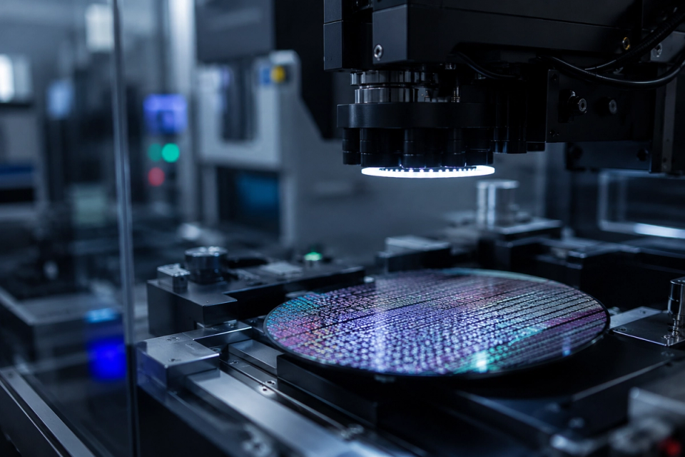
SixSense achieved major semiconductor AI milestones in April, expanding deployments across wafer fabs and backend assembly with measurable yield recovery, ultra-fast AI inspection, and production-scale defect classification. From partnering with Taiwan-based Wavetek Microelectronics Corporation to enabling 0% inspection escapes in high-volume manufacturing, SixSense continues advancing production-grade AI for semiconductor fabs and packaging lines.
Prakriti Chaturvedi22nd Apr 2026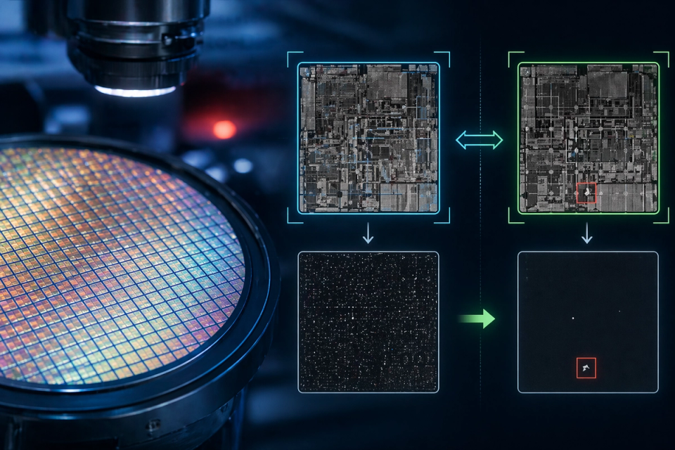
AI-powered sub-pixel die-to-die alignment improves semiconductor inspection accuracy by reducing false positives and boosting yield and throughput at scale.
Sourav Dalai16th Apr 2026
SixSense expanded its semiconductor AI deployments across the US, Taiwan, and Southeast Asia in March 2026, launching real-time embedded inspection systems and scaling AI-driven defect classification for high-volume manufacturing. From SEMI’s Smarter Sensors, Smarter Fabs event in California to advanced packaging deployments and high-throughput AOI inspection in Penang, SixSense continues advancing production-grade AI for semiconductor fabs and OSATs.
Prakriti Chaturvedi27th Mar 2026
AI-powered semiconductor wafer inspection enables real-time, low-latency inline defect detection using edge-based machine learning, model distillation, and dynamic routing to improve yield, throughput, and production efficiency.
Benny Zhen-Peng BIAN26th Mar 2026
SixSense began 2026 by expanding semiconductor AI deployments across Taiwan and global OSAT environments, advancing AI-driven defect classification, wafer sort automation, and real-time probe correction for high-volume manufacturing. From deploying AI-ADC at Tong Hsing Electronic in Taiwan to launching closed-loop AI for wafer test and participating in the GSA Women’s Leadership Initiative in California, SixSense continues scaling production-grade AI across semiconductor fabs and packaging lines.
Prakriti Chaturvedi18th Feb 2026
Semiconductor manufacturing relies on defect detection, pattern recognition, and root cause analysis to manage yield. The challenge lies in retaining experience from past investigations as processes scale. This article explores how knowledge-driven systems support faster and more consistent yield improvement.
Benny Zhen-Peng BIAN12th Feb 2026
AI is reshaping semiconductor demand by shifting industry growth toward higher compute density, memory bandwidth, and system-level integration. AI workloads are driving larger chips, high-bandwidth memory, advanced packaging, and increased use of leading-edge manufacturing nodes. As a result, semiconductor value is concentrating around AI-optimized design, manufacturing, memory, and equipment ecosystems.
Prakriti Chaturvedi10th Feb 2026
India’s semiconductor journey began with early manufacturing ambition in the 1980s, evolved into global design leadership through the 1990s and 2000s, and gained strategic urgency as electronics demand surged. Learning from these phases, India is now rebuilding its semiconductor base around market-relevant manufacturing, packaging, and design integration. With policy alignment, ecosystem thinking, and global engagement, the country is shaping a sustainable role in the global semiconductor landscape.
Prakriti Chaturvedi3rd Feb 2026
The global semiconductor supply chain shifted from the U.S. to Asia to optimize scale, cost, and specialization, creating a deeply interconnected ecosystem. Today, AI-driven demand, supply chain vulnerabilities, and geopolitical risks are pushing the industry to rebalance manufacturing through initiatives like the U.S. CHIPS Act. This shift aims to strengthen resilience while keeping the semiconductor ecosystem global.
Prakriti Chaturvedi30th Jan 2026At micron scales, tiny machine drift can silently erode yield during wafer test. This article shows how AI turns probe marks into real-time feedback, enabling autonomous prober realignment in milliseconds—preventing latent defects, improving uptime, and stabilizing yield as tolerances shrink.
Ayaz Aslam27th Jan 2026SixSense’s AI-ADC platform integrates with inspection and DMS systems to automate defect classification at production scale. Deployed across leading foundries and OSATs, it processes millions of inspection images annually. The platform is now expanding into real-time classification and fab-wide deviation control.
Avni Agrawal22nd Jan 2026Manufacturing downtime is becoming more costly and complex in the Industry 4.0 era. This blog explains how AI-driven root cause analysis helps manufacturers move beyond reactive troubleshooting to identify true causes across inspection, metrology, FDC, and test data. Learn how AI-powered RCA reduces downtime, improves yield, and strengthens overall operational performance.
Vicknes Ratha Kishnan20th Jan 2026
In modern semiconductor fabs, massive amounts of data are generated, yet slow and fragmented decision-making poses the greatest risk as small issues can combine into major yield losses. Traditional automation struggles to provide the context needed to catch these subtle problems early. By connecting and interpreting data intelligently, manufacturers can make faster, smarter decisions and prevent issues before they impact production.
Prakriti Chaturvedi13th Jan 2026
The semiconductor industry now requires real-time, scalable intelligence to manage growing complexity. Sixsense.ai transforms manufacturing data into actionable insights for early detection and proactive control. Trusted globally, it helps fabs and OSATs achieve more with less.
Vicknes Rath Krishnan12th Jan 2026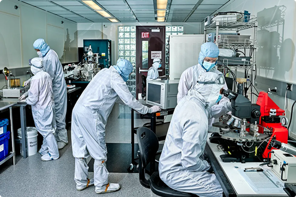
This blog explores how SixSense’s AI-powered defect classification system is transforming semiconductor manufacturing by automating visual inspection and error detection. It demonstrates how advanced AI analytics enhance yield, speed, and reliability—minimizing manual bottlenecks and driving smarter, scalable production.
Nilotpal Nayan5th Dec 2025