

How AI Quietly Reshaped Semiconductor Demand
For decades, semiconductor growth followed a steady and familiar pattern. Computing relied on general purpose processors, manufacturing scaled around predictable volumes, and performance advanced through regular improvements in process technology. Each new generation delivered smaller and more efficient chips that could serve many applications without fundamentally changing how computing systems were organized.
That pattern began to shift as artificial intelligence moved from research environments into real world deployment. In the early 2010s, AI related silicon represented only a very small portion of total semiconductor demand, largely confined to experimental workloads and limited acceleration inside data centers. As AI workloads matured and entered production, they introduced sustained demand for higher compute density, faster access to memory, and tighter coordination across system components. These requirements gradually influenced how chips were designed and how manufacturing capacity was allocated.
This transition also changed how semiconductor growth is measured. Expansion increasingly reflects higher capability and deeper integration within each system, driven by larger processors, faster memory, and tighter interconnects, alongside continued demand across many end markets. By 2025, AI related semiconductors including processors, high bandwidth memory, and networking silicon accounted for nearly one third of total global semiconductor sales, according to Gartner. AI has become a primary driver of industry growth, shaping investment priorities and technology roadmaps across the ecosystem.
From CPU-Centered Computing to Data-Heavy Workloads
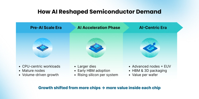
Before AI became a major source of demand, most computing systems relied on CPUs paired with conventional memory. These platforms handled a wide range of tasks efficiently, and semiconductor manufacturing focused on serving broad markets across consumer, enterprise, and industrial applications. Growth during this period came from shipping increasing numbers of chips into an expanding base of devices and systems.
As data volumes grew and machine learning techniques advanced, computing needs began to change. AI workloads require many calculations to run in parallel and depend on rapid access to large datasets. These demands placed pressure on traditional system designs and highlighted the limits of CPU-centric architectures. The shift signaled a gradual change in how silicon would be used inside computing platforms.
AI Workloads Expand the Role of Silicon Inside Each System
As AI adoption increased, the semiconductor market began to change from within computing systems themselves. Training and inference workloads favored parallel architectures capable of processing large volumes of data simultaneously. GPUs and dedicated accelerators moved into central roles within AI platforms, particularly in data centers supporting large-scale models.
These workloads reshaped chip design priorities. Processors grew larger to support higher compute density, and memory moved closer to logic to reduce data movement delays. High-bandwidth memory became a core component of AI systems, supplying data at speeds conventional memory could not match. As a result, AI platforms began to integrate significantly more silicon per system than traditional server designs, combining large logic dies with stacked memory and dense interconnects.
By the mid-2020s, this shift became visible in market results. Gartner reported that AI processing semiconductors generated over $200 billion in revenue in 2025. Growth reflected both expanding deployment and increased silicon content per system, as each AI platform combined advanced logic, memory, and packaging technologies.
Manufacturing and Investment Follow the Workload
As AI models continued to scale, the way chips were built evolved alongside them. These models process vast amounts of data in parallel, placing simultaneous pressure on compute performance, power efficiency, and memory bandwidth. Meeting these requirements pushed manufacturing toward advanced process technologies capable of supporting high transistor density and tighter power control.
This is why advanced manufacturing nodes became central to AI chips. Smaller and more precise transistors allow more computing capability to fit onto a single chip while keeping energy use within practical limits. For foundries, this directly linked process leadership to AI system performance. The ability to manufacture at the most advanced nodes became a key factor in supporting next-generation AI platforms.
Foundries such as TSMC and Samsung play a critical role at this stage of the supply chain by translating complex designs into high-volume silicon. TSMC has indicated that demand for its most advanced nodes is increasingly driven by AI and high-performance computing customers building large accelerators. Samsung has advanced new transistor structures, including gate-all-around designs, to improve power efficiency and performance stability for similar workloads. These manufacturing choices shape how fast and how efficiently AI chips operate at scale.
Memory and packaging grew equally important as AI systems expanded. AI processors depend on constant access to large datasets, making memory speed as important as compute capability. High-bandwidth memory became essential because it delivers data at rates required by modern models. To support this, packaging technologies evolved to place memory closer to processors through 2.5D and 3D integration, allowing logic and memory to function as a tightly coupled unit.
Together, these changes shifted manufacturing priorities from producing individual chips toward building integrated systems. Value increasingly concentrates in the ability to combine advanced logic, high-speed memory, and sophisticated packaging into a single platform, bringing foundries, memory suppliers, and assembly partners into closer coordination.
AI Redefines Where Value Concentrates Across the Stack
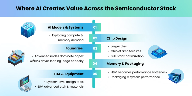
AI-driven demand now flows through every layer of the semiconductor value chain, beginning with large computing systems deployed in data centers. These systems scale compute and memory resources to support training and inference, creating sustained demand for specialized silicon optimized for these workloads.
Chip designers sit at the front of this transformation by translating AI software requirements into hardware architectures. Companies such as NVIDIA, AMD, and Intel focus on processors designed for large-scale parallelism, balancing performance and power efficiency. Larger dies, chiplet-based designs, and close alignment between hardware and software frameworks allow these platforms to scale across different AI applications.
Foundries provide the manufacturing foundation that makes these designs possible. Advanced nodes supported by EUV lithography enable the dense and precise structures required by modern AI accelerators. Equipment suppliers occupy a strategic position here, as their tools directly influence yield, performance, and reliability at high volume.
Memory and packaging suppliers complete the core hardware stack. High-bandwidth memory governs how quickly data moves through AI systems, while advanced packaging determines how efficiently processors and memory interact. Design software and manufacturing equipment support this complexity by enabling system-level modeling, verification, and precision production.
Together, these layers show where value increasingly concentrates within the semiconductor industry. AI shifts emphasis away from standalone components and toward systems built from tightly integrated technologies across design, manufacturing, memory, and equipment.
What This Shift Means for Semiconductor Growth
AI reshaped semiconductor growth by increasing the value embedded within each chip and each system, while overall demand continues across a wide range of applications. Performance requirements, integration depth, and manufacturing precision now guide investment decisions across much of the industry. Capital increasingly flows toward advanced logic, memory, packaging, and equipment aligned with AI workloads.
This shift also carries implications for the global supply chain. Advanced chip design remains concentrated in the United States, while leading-edge manufacturing capacity is anchored in Taiwan and South Korea, with growing investment in the United States, Japan, and parts of Europe. Memory production relies heavily on South Korean suppliers, while advanced equipment and materials draw from a global network spanning the Netherlands, Japan, and the United States. These interdependencies heighten the importance of supply stability and technology access.
Looking ahead, industry roadmaps point toward continued investment in advanced process technologies, new transistor architectures, and deeper integration between logic and memory. Foundries are preparing for further scaling of gate-all-around structures. Memory suppliers are advancing higher-capacity and faster generations of high-bandwidth memory. Packaging providers are expanding hybrid bonding and 3D integration to support increasingly complex systems. EDA and equipment companies continue to align tools around system-level design, process control, and materials innovation.
AI has become a structural force that shapes how chips are designed, how factories are built, and where value accumulates across the semiconductor ecosystem. Understanding this transition offers a clearer view of current market dynamics and the direction the industry is likely to follow in the years ahead.