

There's a strange asymmetry in how modern semiconductor fabs operate.
A 300mm fab moves tens of thousands of wafers a week. An inspection tool flags a defect on a wafer in seconds. A classifier can label a defect in milliseconds. The automated line itself runs at a pace that is precise, fast, mostly hands-off.
And then when something goes wrong, the whole line slows down.
At inspection, a defect signature appears and an SPC chart goes out of control. And suddenly, in the middle of a factory built around speed and repeatability, the most important job becomes a manual investigation that takes anywhere from days to weeks. Defect engineers scramble through loads of data, across spreadsheets and different systems. Lots are held. Tools are stopped, just in case. The fab keeps running, but with one eye half-closed.
This is Root Cause Analysis, and it has long been one of the slowest workflows in semiconductor manufacturing for as long as semiconductor manufacturing has existed. Everything around it has gotten faster. Detection got faster. Classification got faster. Process control got faster. RCA didn't, because an RCA analysis is like finding a needle in a haystack. Finding a suspicious tool among thousands of process tools. Or an underlying cause hidden somewhere in the vast amount of data a fab collects.
That's the part AI is finally able to change.
The Real Problem
If you ask a yield engineer what makes RCA hard, they rarely say "we don't have the data." They have the data. The fab has been collecting lots of granular data for years. But accessing it and analysing it still remains manual and time consuming, dependent on years of tribal knowledge and experience. It's worth understanding why.
A wafer's life in a modern fab is recorded across:
- SPC — the statistical process control system that tracks trends over time. It fires an out-of-control alert as soon as a defect limit is breached.
- MES — the manufacturing execution system, which knows exactly which tool, chamber, recipe, and operator touched each wafer at each step.
- Defect classification systems — which label the defect type and, separately, the spatial pattern on the wafer (an edge ring, a center cluster, a scratch, a streak).
- Equipment logs and FDC traces — fault detection and classification data, which records the second-by-second sensor readings inside each tool: pressures, temperatures, gas flows, RF power, chamber state.
- Maintenance records — preventive maintenance events, recipe changes, qualifications, shift changes.
And many more. Each of these systems was built for its own purpose, by different vendors, over different decades. So the engineer becomes the integration layer. They pull data from different sources, and analyse it in JMP or Spotfire or Excel. Industry estimates put this work at 70 to 80 percent of an investigation's total time. And it's why RCA is slow even in fabs that are otherwise extremely advanced.
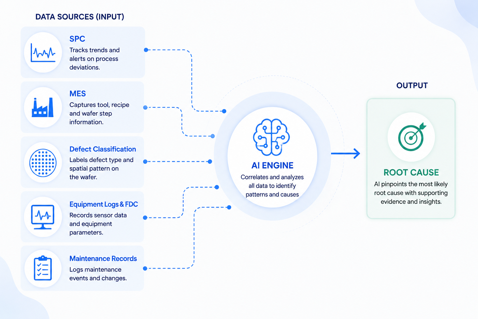
Figure 1: Input sources for AI-RCA (For fabs with some integrated system, it is better for SixSense to get access and pull the data from there
How RCA Actually Plays Out
To make this concrete, let’s take a real case from a recent customer: a residue defect, where 38 wafers were affected across 10 lots. The defect appeared as a streak pattern on the wafer map that often points to a process drift.
The investigation moved through three phases, as follows:
Phase 1 (around six hours). Engineers confirm that the alert is real. The defect count is genuinely out of control. The pre-layer scan was clean, meaning the defect was introduced at the current process step, not carried over from before. A horizontal tool commonality checks if " there is one tool at a single process step that touched every bad wafer?" — but that comes back inconclusive. No single tool at a single process tep was common to all of them.
Phase 2 (around three days). Go deeper. A vertical commonality check across multiple process steps narrows the list to ten suspect tools, then to three based on which ones were active in the right time window. Engineers compare the notch orientation of the affected wafers against the streak direction(the notch is a small mark on the wafer used as a reference point, and the angle of the streak relative to it can tell you something about which direction fluids were moving when the defect was deposited.) They pull FDC traces from suspect tools and compare them against good lots. They look at queue times (how long wafers waited between steps) and metrology SPC for inline thickness. Nothing conclusive yet.
Phase 3 (about a week). Widen the lens. Check for facility events like power fluctuations, chemical delivery anomalies, anything fab-wide that might explain a cluster. Look at CFM (contamination monitoring) data. Pull in past learnings, which usually means a senior engineer remembering "we saw a streak like this in 2022, it was a Clean tool."
Eventually, the answer emerges: a single wet bench tool, at a chemical clean step, where the flow direction matches the streak orientation. Around twenty people had touched the investigation in some way. The total elapsed time was about ten days.
By the time the fix was applied, the lots in question had long since been held or scrapped.
The Costs You See, and the Costs You Don't
The yield loss is the part everyone talks about. It's also the part that's easiest to measure and the least interesting, because it's only one of four costs an RCA delay imposes:
- Yield exposure grows linearly with containment time. Every hour the bad tool keeps running, more wafers pass through it.
- Tool productivity bleeds quietly. When you don't know which tool is bad, the safe move is to stop several suspects. That is additional throughput lost from highly capex intensive tools.
- Engineering capacity gets locked up. The engineers most capable of preventing the next excursion are spending their week investigating the last one. The improvement work that would actually reduce the excursion rate keeps getting deferred.
- Knowledge does not compound. The pattern an experienced engineer recognizes in hour eight of an investigation is, in most fabs, stored exclusively in that engineer's memory. When they move teams or retire, the institutional knowledge over time is forgotten or lost in presentations and reports.
This last one matters more than it seems. A fab's ability to solve excursions quickly depends heavily on a small number of senior engineers who've seen enough cases to pattern-match. That's not a sustainable model, especially as the industry expands faster than it can train people.
What the AI Actually Does
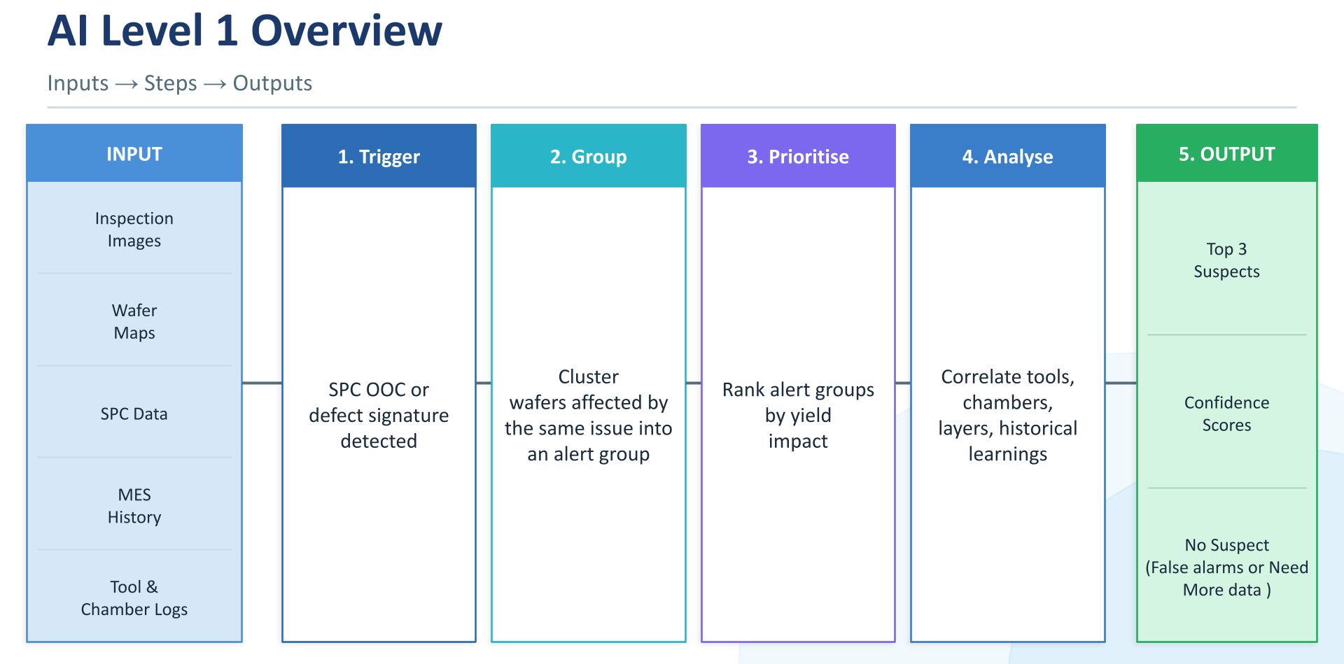
Figure 2: Overview of AI-RCA step-by-step
Once you can give an AI system a unified view of every wafer's complete process history including every tool, chamber, recipe, event, classification, signature, all linked together, the engineer is no longer dealing with huge volumes of data under pressure; the engineer is only reviewing conclusions and making decisions.
The SixSense AI-RCA system runs continuously in the background of the fab. When an SPC violation occurs, a defect signature is detected, or an engineer manually flags an alert, four things happen in sequence, usually within minutes:
It groups the affected wafers intelligently. Not just by lot or scan time, but by the fingerprint of the problem: defect type, spatial pattern, process context, timing. Two wafers showing the same edge-ring residue at the same process step get grouped together even if they came from different lots, because the underlying issue is probably the same. Wafers that look superficially similar but have different fingerprints stay separate.
It maps every wafer's process journey. Each wafer becomes a node in a graph connected to every tool, chamber, recipe, and event it encounters. Connections get weighted statistically: a chamber that processes eight bad wafers and one good wafer scores high; a tool with higher good/bad distribution scores low. Time correlations matter too — a preventive maintenance event four hours before defect onset on a suspect tool adds weight to that connection. 10s of such factors are simultaneously taken into account by AI to eliminate suspects.
It applies process reasoning. The scoring alone isn't enough, because some statistically suspect tools are physically incapable of causing a given defect type. A reasoning layer prunes those out (a PVD tool can't cause a lithography-stage edge-ring), and cross-references the fab's history of past RCAs (streak + clean step has been from wet-bench three times before).
It produces a ranked, explainable shortlist. Typically the top three suspects, each with a confidence score and a plain-language explanation of why it's a suspect: how many bad versus good wafers it touched, what events correlated, what past cases match.
For the residue/streak case above, this entire process took under two hours. The top suspect came back at 0.88 confidence — the same wet bench tool that the ten-day manual investigation eventually identified.
When confidence is high enough, the system can also act directly: hold the affected lots in MES, stop the suspect tool, trigger re-inspection on wafers that passed through it in the same window, and escalate to the right person. Each of these actions has its own configurable confidence threshold, and engineers retain override control at all times. The point isn't to take humans out of the loop. The point is to remove the lag between identification and containment.
What the Numbers Look Like in Practice
It's tempting to read all this as a productivity improvement — a faster way to do an existing job. That undersells what's actually happening. The impact has spanned key Fab metrics as shown in the table below:
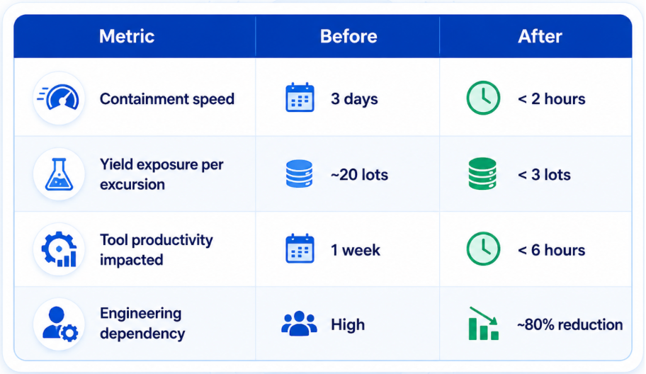
Table 1: Proven ROI with AI-RCA
For the residue case specifically: the estimated yield exposure avoided was around $5 million, and the engineering time saved was about 985 hours on that one investigation alone. Across a quarter's worth of excursions in a typical 300mm fab, the cumulative effect on yield, throughput, and engineering capacity is large enough that it stops being an efficiency story and starts to become that of competitive advantage.
Where This Goes Next: The Path to AI-FDC
The natural next step is AI-FDC — using equipment sensor data to predict yield issues before they show up at inspection or WAT. Catch problems hours earlier, shrink exposure to near zero.
The challenge is signal-to-noise. FDC streams throw off millions of readings per shift; very few matter. A useful detector needs labeled training data with historical FDC patterns linked to the downstream failures they caused. Almost no fab has this in usable form, because creating it means asking senior engineers to manually trace and label past cases.
This is where AI-RCA becomes the foundation. The same system that traces today's excursions is, by construction, generating that labeled dataset. Each investigation produces a clean linkage: defect signature → affected wafers → root-cause tool → time window. Run it across a fab for months and you have hundreds of labeled cases, without disrupting anyone's day job.
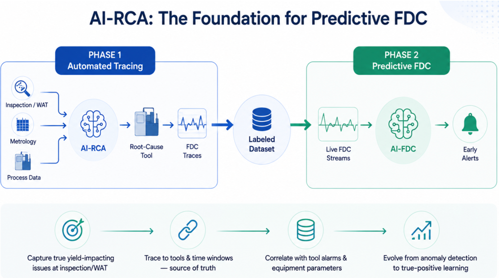
Figure 3: How AI-RCA builds the foundation for Predictive FDC
The roadmap is two phases:
Phase 1 — Automated tracing. AI-RCA in production, links issues at inspection and WAT back to root-cause tools and their FDC traces. Phase 1 ROI stands on its own: sharp drop in investigation headcount, far fewer wrong-tool shutdowns.
Phase 2 — Predictive FDC. Using Phase 1's labels, train models to flag issues from FDC traces ahead of inspection
AI-RCA isn't a destination. It's the foundation that makes the next generation of fab intelligence possible because it solves the labeling problem that has held AI-FDC back for years. Each layer compounds on the one before it. That compounding is the structural shift.