

In most HDD head fabs today, there's a simple inefficiency hiding in plain sight.
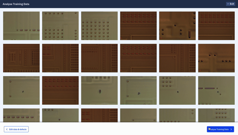
Wafers go through inline optical inspection on AIT. It scans every wafer, captures thousands of defect images, and flags the ones that look problematic. But the optical images are almost never classified. They're captured, and the defect count is used to make an out-of-control decision for a wafer. Next, it's up to the engineers to investigate OOC wafers or recover good sliders that are inked because of cosmetic defects. Increasing demand in the HDD market is putting pressure on the HDD manufacturers to squeeze every possible yield, and in such cases over-inking, false alarms and delayed action on sources of yield loss become costly.
That gap costs far more than most teams realize.
The Way Things Work Today
AIT runs continuously, producing a defect map for every wafer. SPC decides what happens next: if a wafer crosses a defect-count threshold it goes OOC and is held for engineering review; if not, it moves on. Four problems follow from this.

Cosmetic defects flood engineers with false alarms. SPC triggers a hold on defect count alone, and a large share of what AIT flags on a head wafer is cosmetic — stains, residue, minor surface marks — with no effect on read-write performance. Roughly 20 percent of AIT OOC events are cosmetic false alarms. Each one still has to be opened and dispositioned by an engineer, burning review hours on wafers that were never at risk.
Good sliders get over-inked, and the yield is lost. Because the call is made on count rather than defect type, sliders carrying only cosmetic marks get inked alongside the genuinely bad ones. This over-inking runs 1 to 3 percent of otherwise-good dies: pure yield loss that could be recovered.
Critical defects below the OOC threshold are never investigated. SPC works on volume, so a wafer with a handful of low-count, high-severity defects can stay under the threshold and pass. The critical defect is never flagged, the line issue producing it keeps running, and the parts escape downstream into slider fab, HGA and drive build, where they cost far more to catch. The inline escape rate today runs 1 to 2 percent.
Over 80 percent of AIT data is never classified, so baseline yield stays flat. The images from wafers that didn't lead to SPC OOC are never looked at again. Roughly 70 to 80 percent of everything AIT captures goes unused — never turned into the defect-type trends that drive real process control. Without that feedback, baseline yield sits where it always has, around 95 to 96 percent.
What Changes When You Classify at AIT

Classify every defect at AIT and each of those four problems goes away:
Cosmetic false alarms drop, and engineers stop chasing them. Once each defect is classified, cosmetic marks are filtered instead of triggering an SPC OOC alarm. Cosmetic false alarms fall from around 20 percent to below 2 percent with AI. Engineers review far fewer wafers and spend their time on real issues instead of filtering nuisance defects.
Good sliders stop getting inked. With disposition based on defect type rather than count, sliders carrying only cosmetic marks are passed instead of inked. False inking drops from 1–3 percent toward under 0.1 percent — yield recovered directly.
Low-count critical defects get caught and investigated. Classification looks at what each defect is, not just how many there are, so a handful of critical defects becomes a clear signal even when the count stays under the SPC threshold. The issue is flagged and investigated inline, the line problem gets fixed, and the escape rate falls from 1–2 percent toward under 0.2 percent. Unfamiliar signatures route into an "unknown" bin automatically, surfacing emerging issues days or weeks earlier.
Every AIT image feeds process control, and baseline yield moves. Instead of the 20–30 percent used today, the full body of AIT data is classified and turned into defect-type trends. That feedback is what lifts baseline yield from 95–96 percent toward roughly 97 percent — a 1 to 3 point gain.
The Numbers Behind the Story
For a typical mid-to-large head fab, the figures looks like this.

Adding up the value across yield recovery, less over-inking at outgoing quality, fewer escapes into slider and drive assembly, and better labor efficiency, the total comes to somewhere between $7 million and $19 million a year for a fab of this size.
The single biggest driver is yield. Catching an excursion earlier means fewer wafers are exposed to a misbehaving tool before someone hits the brakes. Even a half-point to one-point gain in baseline yield is worth millions when each wafer carries tens of thousands of heads.
Why This Hasn't Happened and How SixSense Solved It
If the value is this clear, why hasn't every fab already done it? Four real obstacles have stood in the way.
1. The defects in images are very small; any escapee is unacceptable
Problem
AIT runs at relatively low optical resolution, so a serious defect can show up as a few faint pixels. A model that classifies these images has to be highly accurate, because the cost of being wrong is steep: labelling a killer as cosmetic could cause escape and therefore models with 0% escape become essential. A model that is only somewhat accurate does more harm than good.
Solution
Architectures built for very small defects. General-purpose vision models are designed for images where the object fills much of the frame, and they tend to lose fine detail deeper in the network — exactly the detail that matters for a defect a handful of pixels wide. SixSense uses architectures that preserve these small features all the way through, so a ten-pixel defect is read as a defect rather than smoothed away as noise.

2. There are no labeled images to learn from
Problem
Fabs keep years of disposition records, but the AIT images themselves are left unclassified by type. There is no ready dataset to train on. Someone first has to define the defect classes and select representative samples for each — slow, expert work that has often not taken up.
Solution
Clustering and unique-image selection make data prep practical. Instead of asking engineers to comb through thousands of raw images one by one, the platform groups visually similar images using unsupervised clustering and surfaces only a few representative samples from each group. An engineer reviews a few hundred well-chosen images instead of tens of thousands of redundant ones, while still covering the full range of defects. Weeks of catalogue creation and labeling come down to hours or days.
3. The product mix is wide and visually varied
Problem
A single inspection layer can cover many head designs, each with its own layout and background pattern. If one model cannot handle all of them, the fab ends up maintaining a separate model per product, and the count quickly grows past what is practical.
Solution
Foundation models that cover hundreds of products in one model. SixSense foundation models are pre-trained on tens of millions of real images across many products, layers and tools. Through that exposure they learn what defects look like in general and how to ignore background noise, which is what lets a single model cover hundreds of product variants at one inspection layer.
4. Cosmetic and critical defects look alike at low resolution.
Problem
A harmless stain and a real surface defect that costs yield can appear almost identical in an optical image. Telling them apart takes a level of precision that earlier AI simply could not deliver at inline speed.
Solution
Context-aware models for the fine distinctions. The hardest cases of cosmetic mark versus real defect require the model to take into account where the defect is located, which layer it is on, what the local pattern looks like, and what has been seen on similar wafers recently, and combines all of it when making a decision.
Together these explain why AIT classification has stayed on most fabs' wish lists rather than in production. What has changed is that AI platforms built specifically for semiconductor and head defect data can now address all four.
Together these four capabilities are what move AIT classification from a research problem to something that runs reliably in production.
The Bigger Picture
This is about treating every piece of inspection data as something to be understood, not just collected. Fabs generate enormous amounts of data every day, and most of it goes unused because there is no scalable way to interpret it in real time. Classification at AIT closes one of the biggest gaps in that pipeline, turning a vast pool of optical images from passive evidence into active intelligence.
The whole disposition loop tightens. Excursions get contained faster. Good dies stop getting inked. Real defects stop escaping downstream. Engineers spend less time investigating noise and more time fixing real problems.
In a line where every hour of delay costs real money and every escaped defect costs even more once it reaches a drive, that is not a marginal improvement. It is a different way of running a fab.
If your team is sitting on AIT optical data that goes un-inspected, or watching cosmetic false alarms drive over-inking while real defects still escape, it is worth asking: what would change if every defect image were classified the moment it was captured?