

AI-powered Auto-Defect Classification
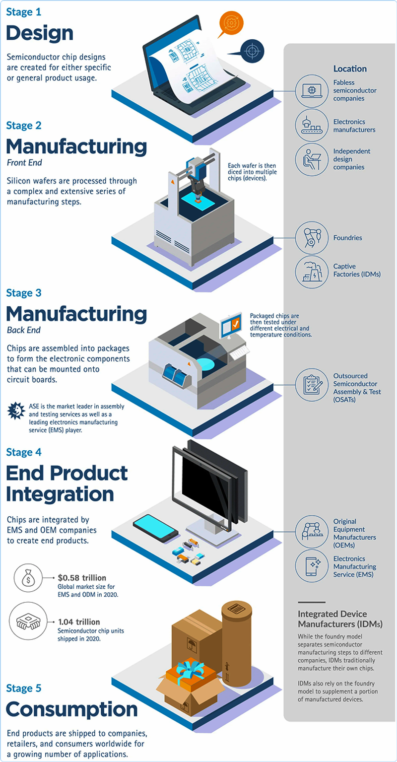
A semiconductor chip’s journey from design to end product is one of the most sophisticated engineering feats in the world—especially for advanced technology nodes like 5nm and 3nm.
It begins at companies like NVIDIA, where engineers translate functionality into intricate chip designs. These designs are then handed over to leading foundries like TSMC or GlobalFoundries, where raw silicon wafers undergo 500–1000 precision-driven process steps over 2–3 months to become fully functional chips.
Each wafer passes through 50–100 inspection steps, ensuring that even the tiniest defects are caught. After fabrication, wafers move to OSAT providers such as ASE or JCET for packaging and testing, before being assembled by companies like Foxconn into devices that power everything from smartphones to cars.
In Integrated Device Manufacturers (IDMs) like Intel or Samsung, this entire journey—from design to packaging—happens under one roof.
But as nodes shrink to 5nm or 3nm, defect density rises, circuit layouts become more complex, and inspection standards must become stricter. For industries like automotive, medical devices, and consumer electronics, there is zero tolerance for error. This is where AI-powered Auto-Defect Classification comes in—enabling fabs to achieve the scale, precision, and speed that manual inspection cannot match.
Yield Challenges in the Semiconductor Industry
Yield is the lifeblood of semiconductor manufacturing. Even a 1% yield improvement can save millions of dollars in wafer costs, reduce waste, and speed up time-to-market. However, despite cutting-edge tools, fabs face persistent yield challenges driven by the complexity of advanced chips.
- Complex Integrated Circuits (IC) Designs
Modern chips involve 3D structures, exotic materials, and nanoscale features. Traditional inspection tools like optical microscopes, Automated Optical Inspection (AOI), and Scanning Electron Microscopes (SEMs) can detect defects but struggle to classify them accurately. Misclassification can delay root-cause analysis and prolong yield ramp-up. - High-Mix, Low-Volume Production
Fabs are no longer producing one or two high-volume products. They now handle hundreds of product variations in small batches. This high-mix, low-volume model complicates automated inspection because inspection recipes must change frequently—making manual review even more error-prone. - Stricter Standards for Automotive and Critical Chips
Automotive chips used in ADAS (Advanced Driver Assistance Systems) or medical devices require near-zero defect tolerance. Even a minor crack or particle could compromise safety, demanding more frequent inspections and far greater classification accuracy than in consumer devices.
Role of Visual Inspection and Defect Classification in Yield
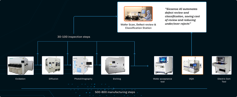
Visual inspection is one of the most powerful levers to improve semiconductor yield. By catching and classifying defects at the right stage, fabs can prevent problems from snowballing downstream. For example, in a typical fab, wafers undergo 50–100 visual inspections during the 500–1000 process steps. For industries like automotive, a seemingly minor scratch, crack, or contamination could disqualify an entire wafer—even if every chip on it still functions.
Defect classification has two primary roles:
- Yield Ramp-Up: During the ramp-up of a new product, fabs must quickly stabilise yield. Accurate classification of critical defects allows engineers to identify yield limiters, trace their root causes, and implement corrective actions fast. This speeds up ramp-up and reduces the cost of early-stage production.
- Process Control: Once production is stable, defect classification ensures real-time process monitoring. By tracking defect trends and correlating them with equipment data, fabs can quickly detect tool-related issues, avoid costly scrap events, and keep equipment running at peak utilization. In short, defect classification is not just a quality gate—it’s a continuous feedback loop that improves manufacturing efficiency and profitability.
Human Errors in Defect Classification: An Industry Bottleneck
Today, most fabs still rely heavily on human operators to review and classify visual defects flagged by AOI systems. But humans have limitations:
- Accuracy ceiling: Human classification accuracy is only 60–70%, leading to missed defects and costly escapes.
- Volume overload: Reviewers inspect millions of defect images annually, leading to fatigue and inconsistency.
- Complex product catalogues: Thousands of products and ever-changing defect patterns overwhelm even experienced operators.
- Fatigue factor: Manual review for 12-hour shifts inevitably leads to errors and slower response times.
Low-skilled labour: Cost pressures often force fabs to rely on operators with minimal training.
With 50+ killer defect types easily confused with 150+ benign defects, this process generates constant escalations to engineers and managers. Every misclassification risks yield loss, line stops, or unnecessary scrapping. In fact, many fabs operate at less than 80% equipment utilization because of false alarms triggered by human misjudgment.
In short: manual defect classification is a bottleneck that drags down productivity, yield, and quality.
How AI Solves This Problem
The Shift from Manual Review to Fab-Level Intelligence
Semiconductor manufacturing has reached a point where human-driven defect classification simply cannot keep up with the complexity of modern nodes. AI-powered classification isn’t just about automating image review—it’s about creating the foundation for fab-level intelligence, where every inspection, every wafer, and every defect feeds into a self-learning system that continuously improves yield, quality, and productivity across the entire fab.
Automation at Scale
AI can process millions of defect images 24/7, applying the same rigorous standards to every wafer without fatigue. By automating classification, fabs eliminate the need for large cleanroom review teams, achieving a 90% reduction in man-to-machine ratio and a 30% faster cycle time.
Zero Escapes and Higher Quality
By learning from historical defect data and continuously validating its predictions, AI reduces human misclassifications and ensures 0% escapes and 12% fewer quality issues. This prevents costly rework, boosts customer confidence, and enhances overall product reliability.
Built for Variety
AI models are trained across hundreds of inspection layers and thousands of product variations, adapting instantly to new designs or process changes. This flexibility allows fabs to scale across high-mix production without weeks of manual recipe updates.
Adaptive Learning for Continuous Improvement
AI systems continuously learn from every new wafer and defect pattern. As the fab introduces new nodes or materials, the AI automatically improves its accuracy—turning every production run into a feedback loop for smarter classification.
Operator Empowerment
By removing the burden of repetitive defect review, AI frees engineers and operators to focus on high-value work like process optimization, yield ramp-up, and equipment tuning, accelerating innovation in the fab.
The Bottom Line
With AI-powered defect classification, fabs achieve measurable operational and financial impact:
- 0.2–2% yield recovery
Through earlier and more accurate defect classification. - 30% faster cycle time
by removing manual review bottlenecks. - 90% reduction
in man-to-machine ratio reducing cleanroom labour requirements. - Higher equipment utilization
by eliminating false alarms and unnecessary line stops. - Significant productivity gains
as engineers focus on root-cause analysis and yield improvement,
not manual reviews. - 0% escapes and 12% fewer quality issues
Improved quality and reliability.
The Vision: From Defect Review to Fab-Level Intelligence
AI defect classification is not the end—it’s the beginning. By turning every inspection into structured, actionable data, fabs build the intelligent backbone for next-generation manufacturing: automated root-cause analysis, predictive yield optimization, and eventually, self-optimizing fabs where production systems adapt in real time.
This is how fabs move from manual defect review to autonomous manufacturing intelligence—and it starts with AI.