

2026 has started with strong progress for SixSense across new deployments in advanced packaging, new applications of AI, and global engagements.
As 2026 begins, we are expanding deployment of our AI-based Automated Defect Classification (AI-ADC) system at Tong Hsing Electronic in Taiwan, strengthening our presence in advanced packaging production. We have also launched a new AI-ADC application in probe testing, enabling real-time probe mark monitoring and closed-loop correction during wafer sort. Alongside these technical milestones, we participated in the GSA Women’s Leadership Initiative hosted by Astera Labs, where our founder Avni Agrawal shared the journey of building SixSense in the semiconductor industry.
At SixSense, we bring AI into fabs and OSATs to help teams act faster when issues arise in high-volume production.
Tong Hsing Electronic Deploys AI-ADC
Tong Hsing Electronic, a leading global semiconductor packaging and test company, has selected SixSense as its AI partner after reviewing multiple solutions. We are deploying our AI-based Automated Defect Classification (AI-ADC) system on their production lines.
Advanced packaging involves complex processes and large volumes of inspection images. Fast and consistent defect decisions are critical.
Our AI automatically analyzes defect images in real time, reducing manual review, improving consistency across shifts, and speeding up decision-making. This supports Tong Hsing’s smart factory roadmap and strengthens inspection stability in high-mix packaging environments.
Please use the translate option in your browser to view it in English: https://www.digitimes.com.tw/tech/dt/n/shwnws.asp?id=0000746587_8GO4PAIB9YHDFI66F5Z7E
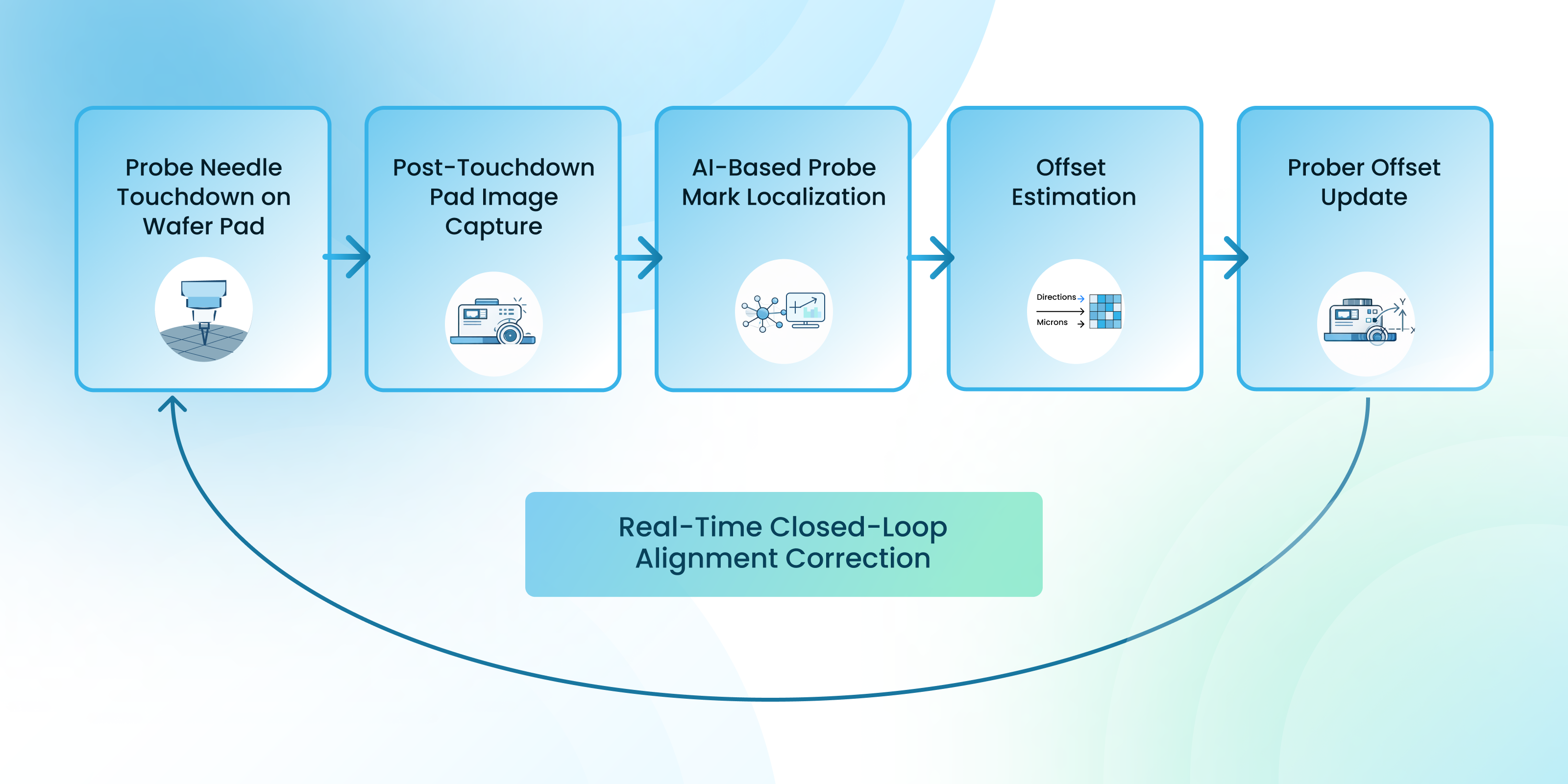
Closed-Loop AI for Wafer Sort and Wafer Test
We also launched a closed-loop AI system for wafer sort and wafer test that monitors probe mark alignment in real time.After every probe touchdown, the system analyzes the image, measures micron-level drift, and sends automatic correction signals back to the probe within milliseconds.
This replaces periodic manual calibration with continuous autonomous control, recovering over 24 hours of tool uptime per week, delivering approximately 1.1% yield improvement, and reducing the risk of latent defects caused by probe drift. This marks a clear step from inspection to autonomous correction in wafer test operations.
Read more:
https://www.sixsense.ai/blog/machine-realignment-using-ai
GSA Women’s Leadership Initiative
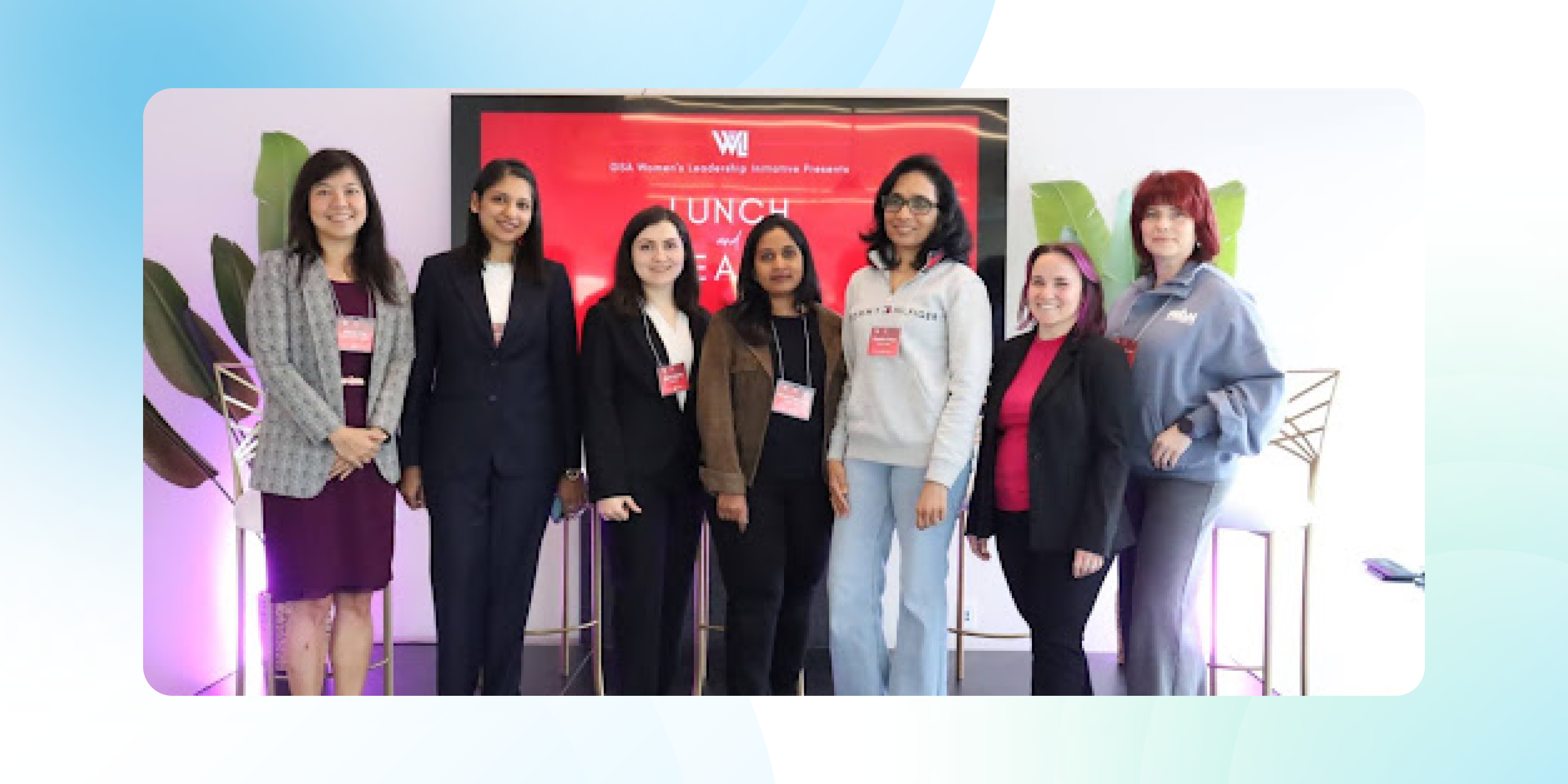
SixSense participated in the GSA Women’s Leadership Initiative session in California, hosted by Astera Labs. Our founder Avni Agrawal delivered a keynote sharing the journey of building SixSense and expanding across Singapore, Malaysia, Taiwan, Israel, and the US.
Her message, “When unfamiliar feels exciting, growth starts to feel like an adventure” resonated strongly. It was a meaningful opportunity to connect with leaders across the semiconductor ecosystem and strengthen our global presence.
Looking Ahead
As we scale AI-ADC adoption, we are moving beyond defect classification to earlier issue detection and faster containment.
By combining classification results with wafer maps and inspection data, we aim to detect repeating patterns earlier, understand how many wafers are affected, and quickly narrow down where the problem started. Instead of waiting for yield loss to appear downstream, teams can act sooner with clearer visibility.
In 2026, our focus is to shorten time-to-action, turning inspection signals into clear decisions that reduce exposure and prevent small process drifts from turning into larger production losses.